
News
A high-tech factory specializing in flow meters
The company's instrument science and technology park covers an area of 100,000 square meters

The company's instrument science and technology park covers an area of 100,000 square meters
STM32F1O3CBT6 | ST | 32-bit ARM Cortex-M3 core general-purpose MCU single-chip microcomputer (F1 medium-density performance line)
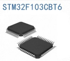
STM32F103CBT6
I. Interpretation of model suffixes
STM32F113: F1 series performance sub-series, Cortex-M3 core, up to 72MHz main frequency
C: LQFP-48 package, 48 pins, body 7mm×7 mm, pin spacing 0.5 mm
B: Flash capacity 128KB; SRAM fixed 20KB (the same package C8T6 is 64KB Flash)
T6: Industrial temperature grade, temperature range ‑40 ℃ ~ + 85 ℃, pallet packaging shipment
Appearance: LQFP-48 square chip, 48 pins around; Chip corner oblique cutting notch mark 1 pin, surface silk printing complete model, batch; Without a bottom pad, the PCB layout needs to reserve enough space for pin pads, and the 0.5mm pitch has certain requirements for the PCB process.
Pin points: 37-way GPIO, most support 5V tolerance; It has a SWD debug interface, a BOOT boot configuration pin, and a VBAT RTC backup power pin.
2. Core electrical parameters
form
parameter
Specifications
kernel
ARM Cortex‐M3, 72MHz, Thumb‑2 instruction set
storage
Flash:128KB;SRAM:20KBSTMicroele...
Power supply voltage
2.0V-3.6V, typical 3.3V power supply STMicroele...
GPIO
37 I/O ports, most 5V tolerant
Communication peripherals
3×USART, 2×SPI, 2×I2C, 1×CAN2. 0B, 1×USB Device full-speed interface
Analog peripherals
2-channel 12-bit ADC, 10 channels, conversion rate 1μs
Timer
7-channel timer with advanced control TIM1, supports PWM output, motor control STMicroele...
Operating temperature
- 40°C to + 85° C industrial grade ST Microelectronics...
Debugging method
SWD / JTAG debugging
Comparison of C8T6: The hardware pins are fully compatible, only the Flash is upgraded from 64KB to 128KB, and the SRAM remains unchanged; CBT6 is the first choice for projects with a large amount of code, storing character sets, and multi-protocol projects.
III. Key Features
The ecology is extremely mature, the data, open-source code, and toolchain are perfect, and it is the classic MCU that is most widely used by domestic engineers.
Built-in CAN, USB, can directly do USB device, CAN bus communication, save external chip.
The high-level timer TIM1 supports complementary PWM output, suitable for motor drive and inverter control scenarios.
RTC real-time clock, support external button battery backup, power off save time and backup register data.
Flash 128 KB, suitable for complex business logic, character set storage, IAP online upgrade.
Non-automotive grade devices, without AEC‑ Q100 certification, cannot be used in official automotive projects.
IV. Typical Application Scenarios
Industrial control: IO acquisition module, small motor drive, sensor acquisition terminal, instrumentation
Consumer Electronics: Smart Home, Smart Door Locks, Small Appliance Controllers, LED Control Systems
Communication conversion: USB-CAN, USB-RS485 converter, DTU terminal master
Educational Development: STM32 Learning Board, DIY Projects, Quadcopter Main Controller
Portable devices, simple BMS, data recorders.
For technical and business consulting, please contact: 182778968089
Welcome to consult, let's start to cooperate!
